Compared with the first generation semiconductor material of silicon (Si) and the second generation semiconductor material of gallium arsenide (GaAs), the third generation semiconductor material (also referred to as wide bandgap semiconductor material) of silicon carbide (SiC) or gallium nitride (GaN) possesses better physical and chemical characteristics while having the features of fast switching speed, small size, high efficiency, fast heat dissipation, etc.
Let us take a look at the new applications derived from the third generation compound semiconductor material:
Autopilot, Augmented Reality, and Robot
Compared with silicon devices, gallium nitride devices emit the laser signal at higher speed and create a 360-degree three-dimensional panorama by the laser/LiDAR system, further improving autopilot, augmented reality, even the development of robots.

Breakthrough in Medical Technology
The third generation semiconductor material can be employed on wireless charging, therefore in addition to the consumer electronics known to all, some of the medical devices may also broaden their fields of usage via wireless charging. For instance, colonoscopy may be conducted by having the examinee swallow an X-ray capsule, and since medical images with 10x or even 100x super resolution can be provided, MRI is able to achieve accurate detection of cancer and disorder at earlier stage. Furthermore, since implantable medical products including cardiac pump, pacemaker, etc. no longer need external power supply, the probability of infection is significantly reduced, so patients would adopt early and their quality of life is enhanced.
5G changes the view on human life
High frequencies such as 5G adopt silicon carbide and gallium nitride that are high voltage resistant, high heat resistant and of high frequency so as to reduce chip area, simplify circuit and lower the need of cooling, and can be used in the field of radio frequency, semiconductor illumination, laser, etc. It can be expected that, in the future, with the help of the commercialization of 5G, the view on human life will be significantly changed.

The typical third generation semiconductor materials of silicon carbide (SiC) and gallium nitride (GaN) have the advantages of high power, high operating temperature, high breakdown voltage, high current density, and high frequency characteristics, which allow significant reduction of chip area and simplification of peripheral circuit design to achieve the goals of reducing modules, system peripheral devices, and the volume of cooling system.
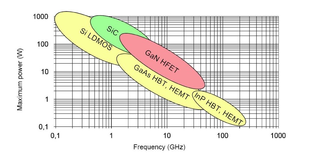
The existing gallium nitride power devices are made from the silicon based gallium nitride and silicon carbide based gallium nitride wafers, wherein the silicon based gallium nitride is likely to be more efficient than the silicon carbide devices as far as area and total cost are concerned and is more suitable for the field of mid-low voltage/high frequency. The comparison chart of working frequency and maximum power for different semiconductor devices is shown below:
The power amplifiers (PA) used on the base stations of the current mobile communication systems are mainly based on the silicon laterally diffused metal oxide semiconductor (LDMOS) technology. However, the LDMOS technology is only applicable to low frequency stage because the bandwidth of LDMOS power amplifier decreases drastically as the frequency increases. The manufacturing process of the LDMOS used for the frequency band of 3.5 GHz is close to its limit. Since the fifth generation mobile communication system (5G) partly adopts higher frequency bands (three major frequency bands are 3.5 GHz, 26 GHz and 28 GHz) in signal transmission to achieve high speed transmission and super low delay capability, LDMOS is getting harder to meet the performance requirements.
Compared with silicon carbide based gallium nitride devices, silicon based gallium nitride devices have an issue of self-heating due to poor heat dissipation on the substrate, which causes a decrease in the performance of gallium nitride transistors, and the silicon based gallium nitride devices are not suitable to be used in an operating environment of high temperature and high frequency. Silicon carbide and gallium nitride have an excellent lattice match, plus the thermal conductivity of silicon carbide material is high (approximately three times as much as silicon), therefore the issue of gallium nitride material having an intrinsically low thermal conductivity is solved, and hence silicon carbide based gallium nitride is advantageous to the application of 5G base station and can be expected to become the mainstream on the market.
Episil Technologies Inc.:http://www.tech.episil.com/